- 您现在的位置:买卖IC网 > Sheet目录17352 > AD588JQ (Analog Devices Inc)IC VREF SERIES PREC ADJ 16-CDIP
�� �
�
�AD588�
��39k� ?�
�+15V�
�tracking� configuration.� A� 100� kΩ,� 20-turn� potentiometer�
�is� used� for� each� trim.� The� potentiometer� for� gain� trim� is�
�connected� between� Pin� 6� (V� HIGH� )� and� Pin� 8� (V� LOW� )� with� the�
�1μF�
�NOISE�
�REDUCTION�
�wiper� connected� to� Pin� 5� (GAIN� ADJ).� The� potentiometer� is�
�adjusted� to� produce� exactly� 10� V� between� Pin� 1� and� Pin� 15,� the�
�amplifier� outputs.� The� balance� potentiometer,� also� connected�
�between� Pin� 6� and� Pin� 8� with� the� wiper� to� Pin� 12� (BAL� ADJ),� is�
�then� adjusted� to� center� the� span� from� +5� V� to� ?5� V.�
�R� B�
�R2�
�A1�
�R1�
�R4�
�R5�
�AD588�
�A3�
�A4�
�+5V�
�–5V�
�Trimming� in� other� configurations� works� in� exactly� the� same�
�+V� S�
�+15V�
�manner.� When� producing� +10� V� and� +5� V,� GAIN� ADJ� is� used�
�to� trim� +10� V� and� BAL� ADJ� is� used� to� trim� +5� V.� In� the� ?10� V�
�and� ?5� V� configuration,� GAIN� ADJ� is� again� used� to� trim� the�
�magnitude� of� the� span,� ?10� V,� while� BAL� ADJ� is� used� to� trim�
�R3�
�A2�
�R6�
�–V� S�
�0.1μF�
�0.1μF�
�SYSTEM�
�GROUND�
�–15V�
�the� center� tap,� ?5� V.�
�Trimming� the� AD588� introduces� no� additional� errors� over�
�temperature,� so� precision� potentiometers� are� not� required.� For�
�single-output� voltage� ranges,� or� in� cases� when� balance� adjust� is�
�not� required,� Pin� 12� should� be� connected� to� Pin� 11.� If� gain�
�adjust� is� not� required,� Pin� 5� should� be� left� floating.�
�SYSTEM�
�GROUND�
�100k� ?�
�20T�
�BALANCE�
�ADJUST�
�100k� ?�
�20T�
�GAIN� ADJUST�
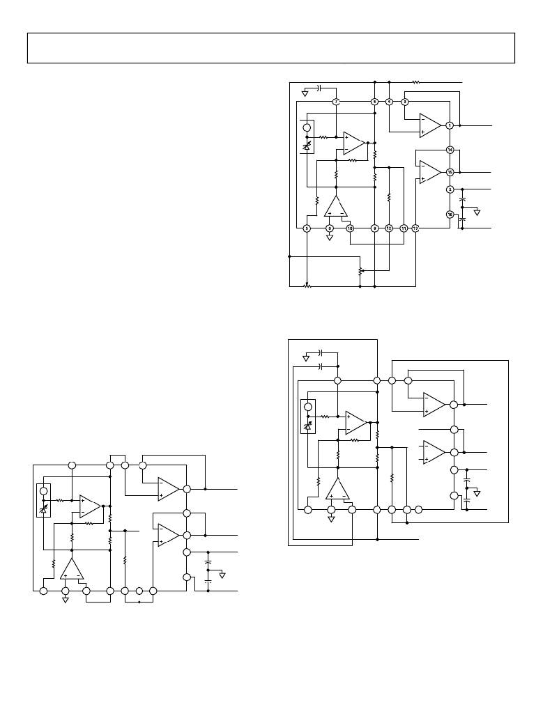
�Figure� 5.� +5� V� and� ?5� V� Outputs�
�In� single� output� configurations,� GAIN� ADJ� is� used� to� trim�
�outputs� utilizing� the� full� span� (+10� V� or� ?10� V),� while� BAL� ADJ�
�is� used� to� trim� outputs� using� half� the� span� (+5� V� or� ?5� V).�
�Input� impedance� on� both� the� GAIN� ADJ� and� BAL� ADJ� pins� is�
�0.1μF�
�NOISE�
�approximately� 150� kΩ.� The� GAIN� ADJ� trim� network� effectively�
�0.1μF�
�7�
�REDUCTION�
�6�
�4�
�3�
�attenuates� the� 10� V� across� the� trim� potentiometer� by� a� factor� of�
�about� 1500� to� provide� a� trim� range� of� ?3.5� mV� to� +7.5� mV� with�
�a� resolution� of� approximately� 550� μV/turn� (20-turn� potentiome-�
�R� B�
�A3�
�1�
�–5V�
�ter).� The� BAL� ADJ� trim� network� attenuates� the� trim� voltage� by�
�a� factor� of� about� 1400,� providing� a� trim� range� of� ±4.5� mV� with�
�A1�
�R1�
�R4�
�AD588�
�14�
�resolution� of� 450� μV/turn.�
�R2�
�R5�
�A4�
�15�
�–10V�
�7�
�6�
�4�
�3�
�+V� S� 2�
�+15V�
�R3�
�R6�
�0.1μF�
�R� B�
�A1�
�R1�
�R4�
�A3�
�1�
�14�
�+10V�
�5�
�9�
�A2�
�10�
�8�
�12�
�11�
�13�
�–V� S� 16�
�SYSTEM�
�GROUND�
�0.1μF�
�–15V�
�SYSTEM�
�R2�
�R5�
�A4�
�15�
�+5V�
�GROUND�
�R3�
�A2�
�R6�
�+V� S� 2�
�AD588�
�–V� S� 16�
�0.1μF�
�0.1μF�
�+15V�
�SYSTEM�
�GROUND�
�Figure� 6.� ?10� V� Output�
�5�
�9�
�10�
�8�
�12�
�11�
�13�
�–15V�
�SYSTEM�
�GROUND�
�Figure� 4.� +10� V� Output�
�Rev.� L� |� Page� 8� of� 20�
�发布紧急采购,3分钟左右您将得到回复。
相关PDF资料
A9BAA-0506F
FLEX CABLE - AFF05A/AF05/AFE05T
RE-2412S/H
CONV DC/DC 1W 24VIN 12VOUT
ESM06DRMN
CONN EDGECARD 12POS .156 WW
AS1323-30 EB
BOARD EVAL AS1323-30
AS1323-27 EB
BOARD EVAL AS1323-27
RE-2409S/H
CONV DC/DC 1W 24VIN 09VOUT
EGM06DRMN
CONN EDGECARD 12POS .156 WW
LQW2UAS12NJ00L
IND 12NH 1000MA SRF 3300MHZ 1008
相关代理商/技术参数
AD588KQ
功能描述:IC VREF SERIES PREC ADJ 16-CDIP RoHS:否 类别:集成电路 (IC) >> PMIC - 电压基准 系列:- 标准包装:2,000 系列:- 基准类型:旁路,可调节,精度 输出电压:1.24 V ~ 16 V 容差:±0.5% 温度系数:- 输入电压:1.24 V ~ 16 V 通道数:1 电流 - 阴极:100µA 电流 - 静态:- 电流 - 输出:20mA 工作温度:-40°C ~ 85°C 安装类型:通孔 封装/外壳:TO-226-3、TO-92-3(TO-226AA)成形引线 供应商设备封装:TO-92-3 包装:带卷 (TR)
AD588SD
制造商:未知厂家 制造商全称:未知厂家 功能描述:Voltage Reference
AD588SD/883B
制造商:未知厂家 制造商全称:未知厂家 功能描述:Voltage Reference
AD588SE
制造商:Rochester Electronics LLC 功能描述:- Bulk
AD588SE/883B
制造商:Analog Devices 功能描述:V-Ref Programmable ±5V/±10V 20-Pin LCC Tube
AD588SQ
制造商:Rochester Electronics LLC 功能描述:IC - PROGRAMMABLE V REF. - Bulk
AD588SQ/883B
制造商:Rochester Electronics LLC 功能描述:IC - PROGRAMMABLE V REF. - Bulk
AD588TD
制造商:未知厂家 制造商全称:未知厂家 功能描述:Voltage Reference